
Answer:
Silicon single crystal wafer containing dopants with a thickness of less than 1μm.

CCMC is committed to becoming one of the main suppliers of semiconductor silicon wafers in the world, breaking the long-term foreign monopoly on the domestic semiconductor silicon wafer market, and realizing the true "Chinese smart manufacturing" in the semiconductor silicon material industry.
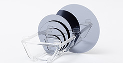
The semiconductor silicon wafers of CCMC have various specifications, different material characteristics and surface treatment methods.
From now on, describe the wonderful moments of CCMC. Every moment will become a historical milestone.

Silicon single crystal wafer containing dopants with a thickness of less than 1μm.
Firstly, the silicon ore is purified to prepare polysilicon, and then the polysilicon is mixed with the dopant to melted and recrystallized to prepare a single crystal ingot. Finally, after ingot slicing, beveling, lapping, donor kill, polishing, cleaning and other operations, silicon wafers with high flatness and surface cleanliness are prepared.
Wafers are mainly used in various semiconductor chips, and then used in various electronic devices in daily life through various assembly, such as: TVs, computers, mobile phones, cars, etc.
1. The reserves of silicon on the earth reach 26.8%, second only to oxygen;
2. The energy gap of silicon is large (1.13V), which makes it have a higher operating temperature and lower leakage current;
3. The SiO2 layer on the surface of the silicon wafer can withstand high temperature and protect the silicon wafer.
Silicon often exists in rocks, dust, and sand in the form of compounds (such as silicate, silicon dioxide).
The dopants are mainly boron (B), phosphorus (P), arsenic (As), and antimony (Sb). Among them, the B doped silicon wafer is P-type, which is mainly hole-conducting. P, As, and Sb doped silicon wafers are N-type and use electrons to conduct electricity.