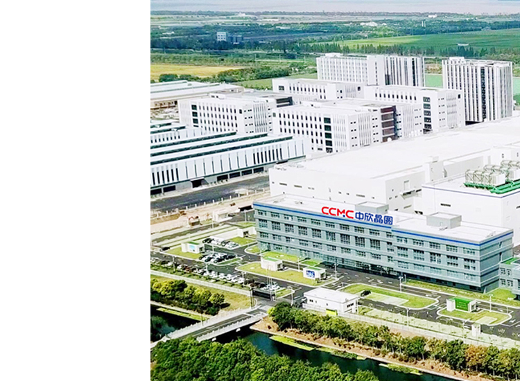
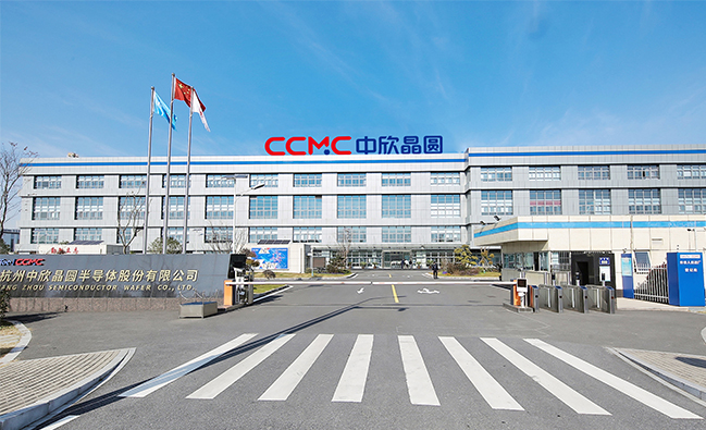
About CCMC
Company Profile 
President Speech
Corporate Concept
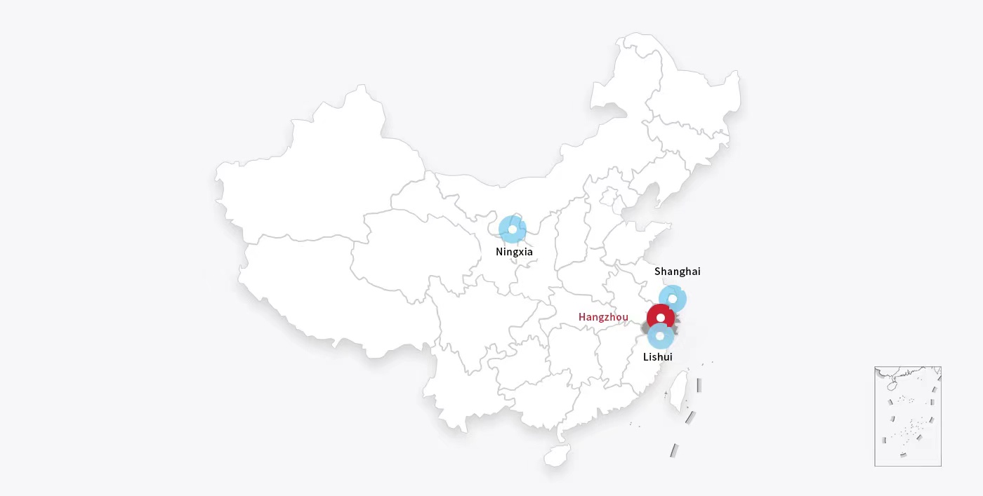
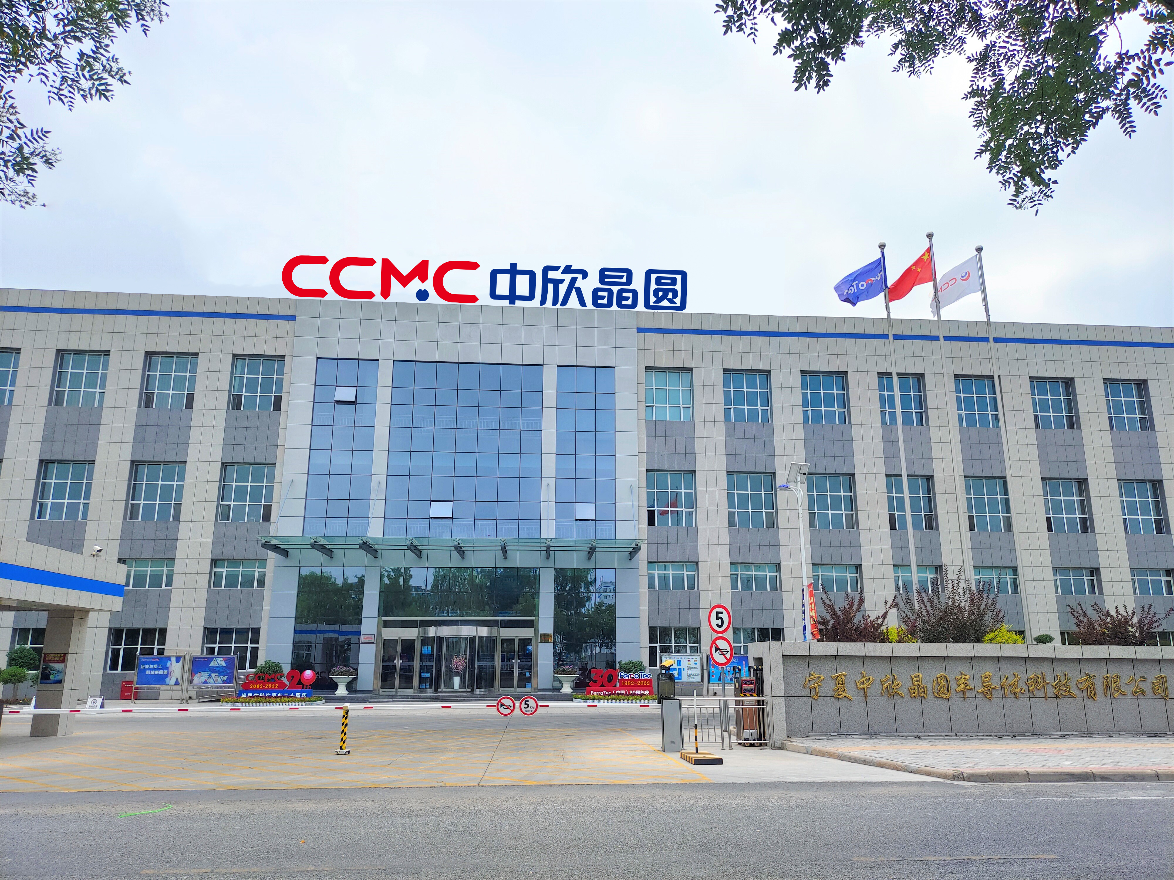
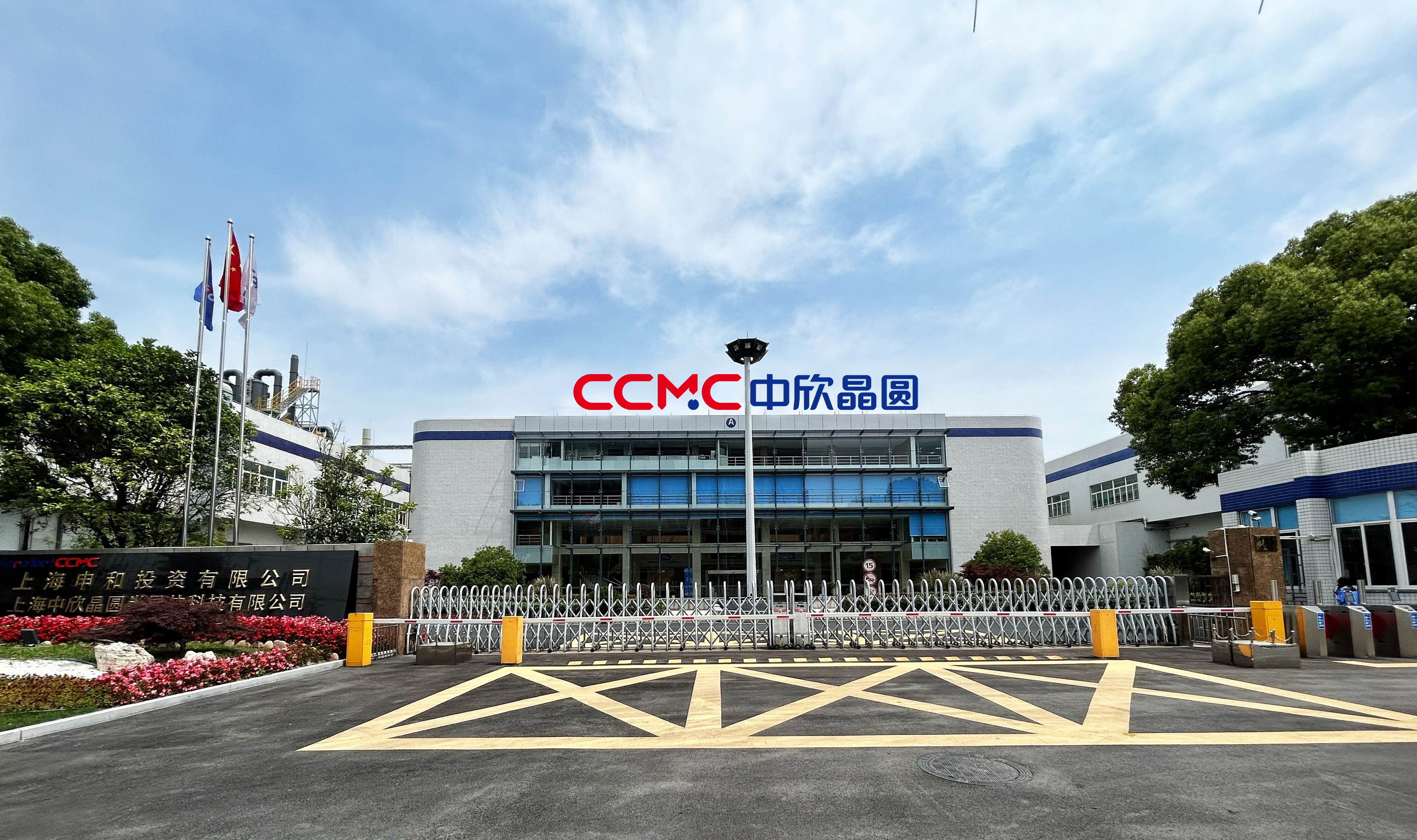
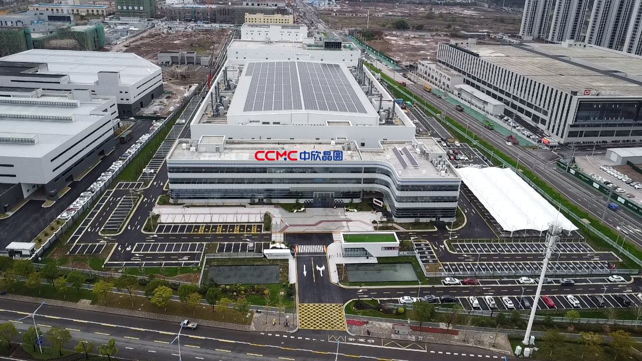
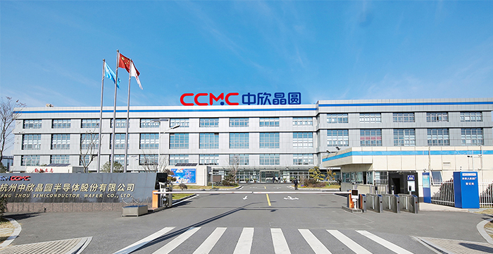
Service Location
Development History
Customer Commitment
Team Building
About CCMC
CCMC is committed to becoming one of the main suppliers of semiconductor silicon wafers in the world, breaking the long-term foreign monopoly on the domestic semiconductor silicon wafer market, and realizing the true "Chinese smart manufacturing" in the semiconductor silicon material industry.
Products and Technology
About semiconductor silicon wafers
List of Semiconductor Products
Manufacturing Methods of Semiconductor Wafers
Manufacturing Capabilities and Technical Advantages
Q&A about Silicon
Download Center
Products and Technology
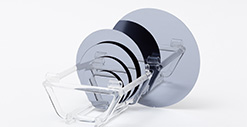
The semiconductor silicon wafers of CCMC have various specifications, different material characteristics and surface treatment methods.
News Center
News Center
From now on, describe the wonderful moments of CCMC. Every moment will become a historical milestone.
Human Resources
Human Resources
Contact Us
Contact Us